
Eliminating the connector and keeping the connection
Lattice Semiconductor Corporation has announced the expansion of its Lattice Snap wireless connector product family to support broader adoption of 60GHz wireless technology in consumer and embedded applications.
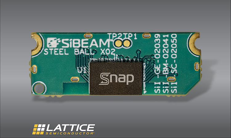
The new Lattice Snap modules, based on Lattice’s SiBEAM 60GHz technology, enables manufacturers to easily integrate short range, high speed 60GHz wireless links into their products. To simplify the design process further, Lattice has included the Snap modules, which are compliant with regulatory requirements in several jurisdictions, into their Snap evaluation kit for fast prototyping and time-to-market. Electronic Specifier Editor Joe Bush spoke to Abdullah Raouf, Senior Product Marketing Manager for Lattice Semiconductor, prior to the launch of the modules.
The Snap technology from Lattice has actually been around since 2016 but with the launch of its new module, Lattice are aiming to expand its reach to more customers while at the same time offering an easier design cycle when using the Snap technology.
However, prior to discussing the new modules, Raouf spoke a little bit about the need to go wireless in the first place.
Why go wireless?
He commented: “Snap technology is a wireless technology and by going wireless you are essentially removing connectors from the design of mobile devices. This leads to a more robust design, and an improved, thinner look and feel (one of the main reasons that limit thin phone design is the connector and we are seeing a trend where connectors are being removed, for example it’s now very rare to find a 3.5mm jack in a mobile phone).
“The next step is to remove the USB connector, and this is where we are trying to offer a solution – eliminating that USB connector completely, and thereby offering an improved user experience.”
More than one way to go wireless
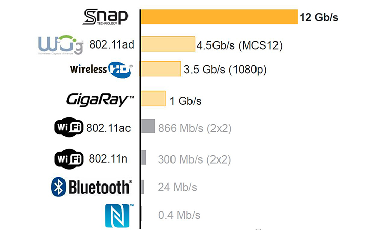
Snap technology is not the only route to wireless. There are a range of different technologies out there for routing wireless between two systems (see below) – ranging from 0.4Mb/s right up to 4.5Gb/s which can be achieved with WiGig.
However, as Raouf explained, Snap offers a 12Gb/s wireless link which has mobile in mind. “This means we wanted to increase the speed but not the power. So despite the speed we are achieving, Snap Technology is very competitive in terms of power in comparison with the other available technologies. The main reason for that is that we are targeting a very short range wireless technology.”
There are other non-standard competing technologies available, however Raouf went on to state that these only offer half of what Lattice offer i.e. a single direction, single chip type solution. “We offer a complete bi-directional link,” he said. “Which means signals in each direction with a single chip. If you add more than one chip together from competing solutions you can get up to the data rates that we’re talking about, but we’re the only true single chip solution on the market.”
What is snap?
The short range connection of Snap Technology looks and feels like a standard connection with a connector and cable. The difference is that nothing gets inserted as there are no holes into the device. It’s a completely closed off connector, with the two connectors aligned via magnetics or via industrial design. The maximum distance between the two chips is around one centimetre.
Raouf continued: “What we’re doing is trying to eliminate the USB 3.1, USB 2.0 and I2C signals. These are generally electrical signals that get driven to a mechanical connector, but we’re converting that electrical signal to a wireless signal. There is no software or drivers needed. You place the two chips into your system and as soon as they are within close enough proximity the link is established.”
Conventional Connectivity
In a conventional connectivity solution you would have a USB cable that connects two systems. You would also need something like I2C protocol communication between the systems, and that would require another cable. “So, that’s two systems and two cables,” said Raoud. “With Snap you can eliminate all of that but still maintain the link. The application processor will only see the USB hub. Just as it doesn’t see the mechanical connector it will also not see the Snap Technology. So that means that whatever happens on the USB end points, the Snap Technology does not upset it in any way.”
The benefits (see below)
Improved industrial design: The placement of the connector is now very flexible. In the past most phones would feature the connector on the bottom which has become the norm. However, with Snap you can place the connector anywhere.
Improved user experience: Now you can connect accessories or data transfer techniques a lot easier. Nothing needs to be plugged-in. All you need to do is align the two end points and the link is established.
Improved robustness: Connectors have lifetimes and the more you plug them in and take them out the closer they are to failure – whether it has 5,000 or 10,000 mating cycles, they will fail eventually. With the non-mechanical solution that Snap Technology is offering, that point of failure is eliminated.
Improved cost effectiveness: Every connector you have is a window into the outside world, so you not only have to take into consideration the cost of the connector itself but you also have to provide ESD protection on every single pin. With Snap you are saving on that ESD protection, and the price of the mechanical connector itself. There is of course a cost associated with the Snap Technology but you are getting more value as there are more use cases for the end customer.
Environmental proof: It goes without saying that the fewer mechanical connections the less access outside influences have on the device. Snap Technology therefore provides protection from factors like dust and water.
Target applications (see below)
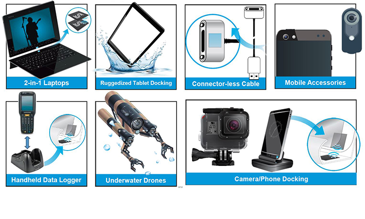
Snap replaces a USB connector so can essentially go anywhere that you currently see a USB connector, meaning the list of potential applications is extensive. However, the key applications that are of particular focus for Lattice include 2-in-1 laptops, ruggedised tablet docking, connector-less cable, mobile accessories, handheld data loggers, underwater drones and camera/phone docking.
Raouf added: “In these areas Snap has already had some success. In fact nobody is in as many products in production as Lattice. We have shipped far more units for this type of short range high speed data technology than anyone else in the world.”
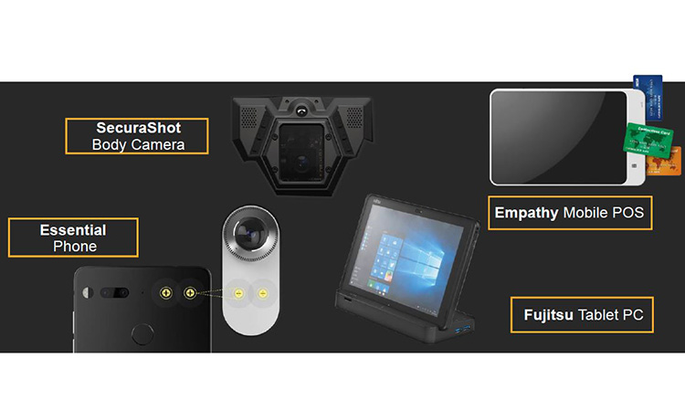
Some of Lattice’s Snap Technology design wins include:
Essential phone: This has a click connect link which enables you to route USB 3.0 and USB 2.0 signals wirelessly. The phone has a 360° camera which can attach very easily to the phone to achieve a USB connection.
SecuraShot Body Camera: This is worn by police officers and is required to be worn for an eight to ten hour shift while operating off of the battery. Therefore, the company needed a low power technology that could take all of the captured data (around 200Gbs) throughout the day and transfer it to a PC very easily for further analysis.
Empathy Mobile POS: This company is targeting an environmentally rugged type POS device that will be operated by service staff handling food and drink etc. Obviously in these sorts of applications spills can occur, so they wanted a connection-less design that would eliminate the ingress issue that would occur in the event of a spill, as well as provide an added layer of security. Roauf added: “There is credit card information stored inside POS terminals so you don’t want someone to be able to connect a USB dongle and view that information. With Snap the USB connector is hidden.”
Fujitsu Tablet PC: This provides an example of how easy Snap Technology makes device docking - improving the user experience. “You don’t have to align anything, you just drop the tablet into the dock, everything is aligned automatically and the link is established - allowing you to have USB data going from the tablet to the dock,” said Raouf.
Problems have occurred
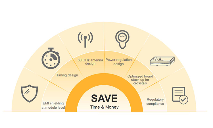
However, since the introduction of Snap Technology there have been some issues that have arisen, creating some challenges with regards to system design.
“We found that the amount of knowledge that our customers tended to have when designing products was limited when it came to material, cross talk and interference effects, plus regulatory compliance. This caused the development time for our customers to be a lot longer than they originally wanted,” Raouf continued.
Solution
Lattice needed to significantly reduce the development time for its customers, and as result has introduce the Snap Module. This module provides a completely regulatory compliant solution in which Lattice has optimised cross talk and interference and made sure that all the test results and data on different materials has been provided.
Raouf added: “Not only are we offering this module turnkey solution but we’re also consolidating all of our data into an easy to understand document where our customers can take the information, shape the module and design quickly.”
A prime example of this in action would be the application previously mentioned with SecuraShot. When the company approached Lattice enquiring about the technology, rather than using the chip, Lattice suggested they try out the module. Within a month the company had a working prototype, significantly reducing the design-in time.
“This is what our customers have been asking us for,” said Raouf. “At the end of the day, designing with wireless is hard and customers don’t want to spend extra time and effort designing a system – it just doesn’t make sense for them. So now that we are able to reduce that design time we are going to be able to reach a lot more customers.”
Raouf explained that just working out what sort of material to use on a product can take a few months of effort in itself, so by following the Lattice Module guidelines, the customer kind find out exactly what material they need and at what thickness. Crosstalk and interference has also been improved.
In addition, regulatory compliance is something that can be a minefield when it comes to product design. Raouf added that many of Lattice’s customers simply don’t understand the compliance requirements, and so cannot perform any pre-testing. As such they would have to go to a certification lab, and if their product fails, they would have to go back and forth until they achieved a pass. This would obviously cost time and money.
He added: “The regulatory lab doesn’t tell you why you’re failing, or how to improve. They don’t provide you guidance, they just tell you if you’ve passed or failed. So because we’re providing a module that’s fully regulatory certified, our customers don’t even have to think about it.”
Available modules
Lattice has released four brand new products to the market – MOD6210, MOD6212, MOD6211, MOD6213 – and a customer can choose these parts based on their application, but regardless of the module Raouf identified that there are significant time to market benefits.
Time-to-market benefits
He added: “Beforehand, the Snap Modules were not broadly available, it was only the ICs. And because of the limited knowledge, even when we said the ICs were available, a lot of customers couldn’t really design it into their projects. So this module is not only going to allow a quicker time to market it will enable a lot more customers to design with this technology.
“The Snap Modules also provide considerable BOM improvement. We’ve included the crystal design which has been matched to our IC, the power regulation has been included with an optimum power-to-noise ratio, and the antenna is built-in. Because of this the customer doesn’t need to worry about additional BOM requirements. All they need to do is follow the guidelines with regards to the recommended enclosure material and thickness, provide a single 3.3V power rail and the USB signals, and that’s it.
“We’re trying to offer a very simple plug-and-play type solution and the key value to our customers is improved time and money – quicker design cycle and quicker time to market – achieved by lower design cost via the elimination USB connectors. And with the modules we are now able to eliminate more end application USB connectors, enabling us to approach much smaller companies who we weren’t able to work with in the past. The new Snap modules not only accelerate time to market, but will enable 60GHz technology to be easily integrated into broader consumer and industrial products.”
Product Spotlight
APV1111GVY
Panasonic

Panasonic PhotoMOS® Photovoltaic MOSFET High-Power Drivers
| SKU: | |
|---|---|
| Stock: | 3490 |
| Cost: | $3.95 |
