
Small changes; big differences
As next-gen 5G systems will be complex to design, developers should seek out devices that have built-in functionality to help make the job easier.
Upcoming 5G wireless communications systems will likely be required to support much wider bandwidths (200MHz and larger) than the 4G systems used today, along with large antenna arrays, enabled by higher carrier frequencies, that will make it possible to build much smaller antenna elements. These so-called massive MIMO applications, together with more stringent latency requirements, will increase design complexity by an order of magnitude.
Moving to 20nm not only enables the higher integration capabilities, improved fabric performance and lower power consumption that come with any geometry node migration, but greatly enhanced features that directly support DFE applications. For example, a complete 8Tx/8Rx DFE system with instantaneous bandwidth of 80-100MHz can fit in a single midrange UltraScale FPGA, while a two-chip solution is necessary on the 7 Series architecture.
Xilinx has significantly increased the clocking and routing resources in the UltraScale architecture which enables higher device utilisation, especially for high-clock-rate designs. In effect, routing congestion is reduced and designers can achieve better design packing and LUT utilisation; in particular, LUT/SRL compression is more efficient. This is an interesting fabric feature that users can exploit to better pack their designs and consequently optimise resource utilisation as well as dynamic power consumption, which can be reduced by a factor of up to 1.7 for the related logic.
The clocking architecture and Configurable Logic Block (CLB) also contribute to better device utilisation in the UltraScale devices. Although the CLB is still based on that of the 7 Series architecture, there is now a single slice per CLB (instead of two), integrating eight, six-input LUTs and 16 flip-flops. The carry chain is consequently 8 bits long and a wider output multiplexer is available. In addition, Xilinx has also increased the control-set resources (that is, the clock, clock-enable and reset signals shared by the storage elements within a CLB).
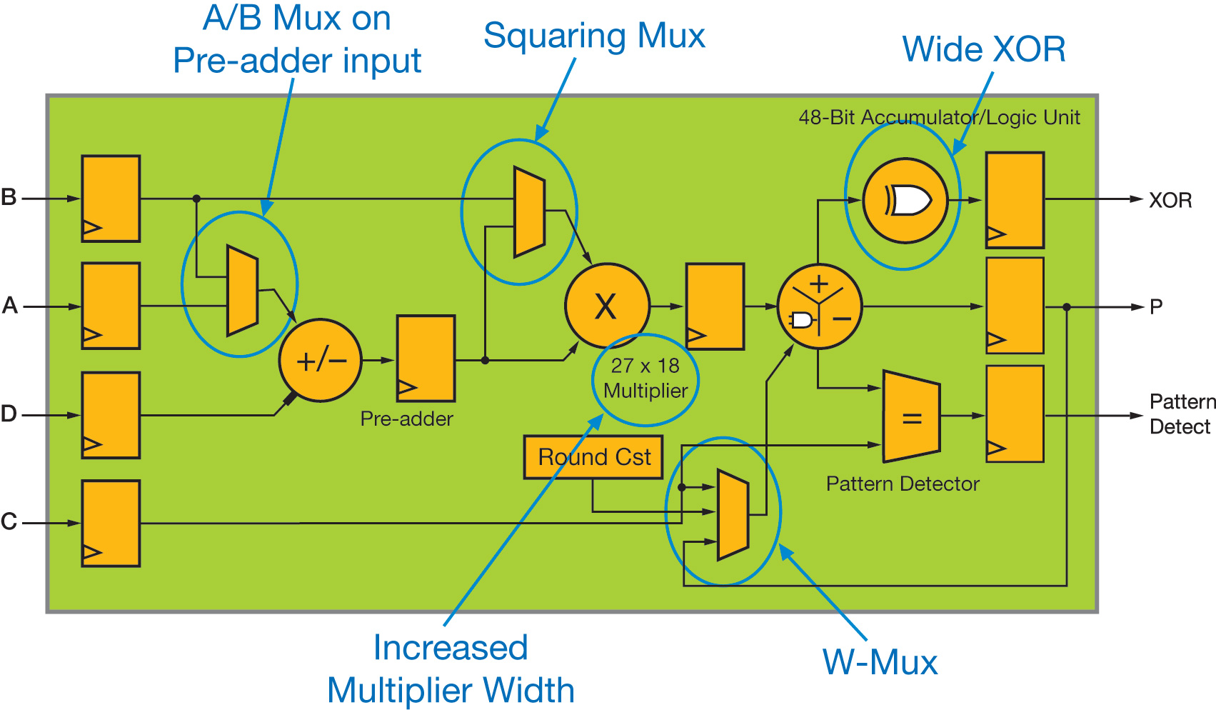
Figure 1 - High-level functional view of the UltraScale DSP48 slice
However, it is essentially the improvements to the DSP48 slice and Block RAM that have the most impact on radio design architectures. Figure 1 highlights the functional enhancements compared with the 7 Series slice (DSP48E1).
Floating-point support
Increasing the multiplier size from 25x18 to 27x18 has minimal impact on the silicon area of the DSP48 slice, but significantly improves the support for floating-point arithmetic. First, it is worth pointing out that the DSP48E2 can in effect support up to 28x18-bit or 27x19-bit signed multiplication, achieved by using the C input to process the additional bit.
This makes it possible to implement a 28x18-bit multiplier with a single DSP48E2 slice and 18 LUT/flip-flop pairs. The same applies for a 27x19-bit multiplier, using 27 additional LUT/flip-flop pairs. In both cases, convergent rounding of the result can still be supported through the W-mux.
A double-precision floating-point multiplication involves the integer product of the 53-bit unsigned mantissas of both operators. Although a 52-bit value (m) is stored in the double-precision floating-point representation, it describes the fractional part of the unsigned mantissa, and it is actually the normalised 1+m values, which need to be multiplied together, hence the additional bit required by the multiplication. Taking into account the fact that the MSBs of both 53-bit operands are equal to 1, and appropriately splitting the multiplication to optimally exploit the DSP48E2 26x17-bit unsigned multiplier and its improved capabilities (e.g., the true three-input 48-bit adder enabled by the W-mux), it can be shown that the 53x53-bit unsigned multiplication can be built with only six DSP48E2 slices and a minimal amount of external logic.
The 27x18 multiplier of the DSP48E2 is also very useful for applications based on fused data paths. The concept of a fused multiply-add operator has been recently added to the IEEE floating-point standard. Basically, it consists of building the floating-point operation A*B+C, without explicitly rounding, normalising and de-normalising the data between the multiplier and the adder. These functions are indeed very costly when using traditional floating-point arithmetic and account for the greatest part of the latency. This concept may be generalised to build sum-of-products operators, which are common in linear algebra (matrix product, Cholesky decomposition). Consequently, such an approach is quite efficient for applications where cost or latency are critical, while still requiring the accuracy and dynamic range of the floating-point representation. This is the case in radio DFE applications for which the digital pre-distortion functionality usually requires some hardware-acceleration support to improve the update rate of the nonlinear filter coefficients. You can then build one or more floating-point MAC engines in the FPGA fabric to assist the coefficient-estimation algorithm running in software (e.g. on one of the ARM Cortex-A9 cores of the Zynq SoC).
For such arithmetic structures, it has been shown that a slight increase of the mantissa width from 23 to 26 bits can provide even better accuracy compared with a true single-precision floating-point implementation, but with reduced latency and footprint. The UltraScale architecture is again well adapted for this purpose, since it takes only two DSP48 slices to build a single-precision fused multiplier, whereas three are required on 7 Series devices with additional fabric logic.
The pre-adder, integrated within the DSP48 slice in front of the multiplier, provides an efficient way to implement symmetric filters that are commonly used in DFE designs to realise the digital upconverter and downconverter functionality.
Fourth input
It is indisputably the addition of a fourth input operand to the ALU, through the extra W-mux multiplexer, which brings the most benefit for radio applications. This operand can typically save 10 to 20% of the DSP48 requirements for such designs compared with the same implementation on a 7 Series device.
The W-mux output can only be added within the ALU (subtraction is not permitted), and can be set dynamically as the content of either the C or P register or as a constant value, defined at FPGA configuration (e.g. the constant to be added for convergent or symmetric rounding of the DSP48 output), or simply forced to 0. This allows performing a true three-input operation when the multiplier is used, such as A*B+C+P, A*B+C+PCIN, A*B+P+PCIN, something that is not possible with the 7 Series architecture. Indeed, the multiplier stage generates the last two partial-product outputs, which are then added within the ALU to complete the operation. Therefore, when enabled, the multiplier uses two inputs of the ALU, and a three-input operation cannot be performed on 7 Series devices. Two of the most significant examples that benefit from this additional ALU input are semi-parallel filters and complex multiply-accumulate operators.
Linear filters are the most common processing units of any DFE application. When integrating such functionality on Xilinx FPGAs, it is recommended, as far as possible, to implement multichannel filters for which the composite sampling rate (defined as the product of the number of channels by the common signal-sampling frequency of each channel) is equal to the clock rate at which the design is running. In a so-called parallel architecture, each DSP48 slice supports a single filter coefficient per data channel, which greatly simplifies the control logic and hence minimises the design resource utilisation.
However, with higher clock-rate capabilities (for example, more than 500MHz on lowest-speed-grade UltraScale devices), and for filters running at a relatively low sampling rate, it is often the case that the clock rate can be selected as a multiple of the composite sampling rate. It’s desirable to increase the clock rate as much as possible to further reduce the design footprint, as well as the power consumption. In such situations, a semi-parallel architecture is built where each DSP48 processes K coefficients per channel, where K is the ratio between the clock rate and the composite sampling rate. The most efficient implementation then consists of splitting the filter into its K phases, each DSP48 processing a specific coefficient of these K phases.
At each clock cycle, the successive phases of the filter output are computed and need to be accumulated together to form an output sample (once every K cycle). Consequently, an additional accumulator is required at the filter output compared with a parallel implementation. This full-precision accumulator works on a large data width, equal to bS+bC+bF, where bS and bC are respectively the bit widths of the data samples and coefficients, and bF=Log2N is the filter bit growth, N being the total number of coefficients. Normal practice is therefore to implement the accumulator within a DSP48 slice to ensure support for the highest clock rate while minimising footprint and power.
 and UltraScale (below) architectures.jpg)
Figure 2 - Implementation of a semi-parallel filter on 7 Series (above) and UltraScale (below) architectures
It should be noted that semi-parallel architectures can be derived for any type of filter: single-rate, integer or fractional-rate interpolation and decimation. Figure 2 shows a simplified block diagram for both 7 Series and UltraScale implementations. It clearly highlights the advantage of the UltraScale solution, since the phase accumulator is absorbed by the last DSP48 slice thanks to the W-mux capability.
It is well known that you can rewrite the equation of a complex product to use only three real multiplications. By exploiting the built-in pre-adder, you can implement a complex multiplier with three DSP48s only; one to compute P1 and the other two to handle the PI and PQ outputs. Depending on the latency requirements, which also dictate the speed performance, some logic needs to be added to balance the delays between the different data paths. To get maximal speed support, the DSP48 must be fully pipelined, which results in an overall latency of six cycles for the operator. A two-cycle delay line is consequently added on each input to correctly align the real and imaginary data paths. Those are implemented with four SRL2 per input bit, which are in effect packed into two LUTs by taking advantage of the SRL compression capabilities.
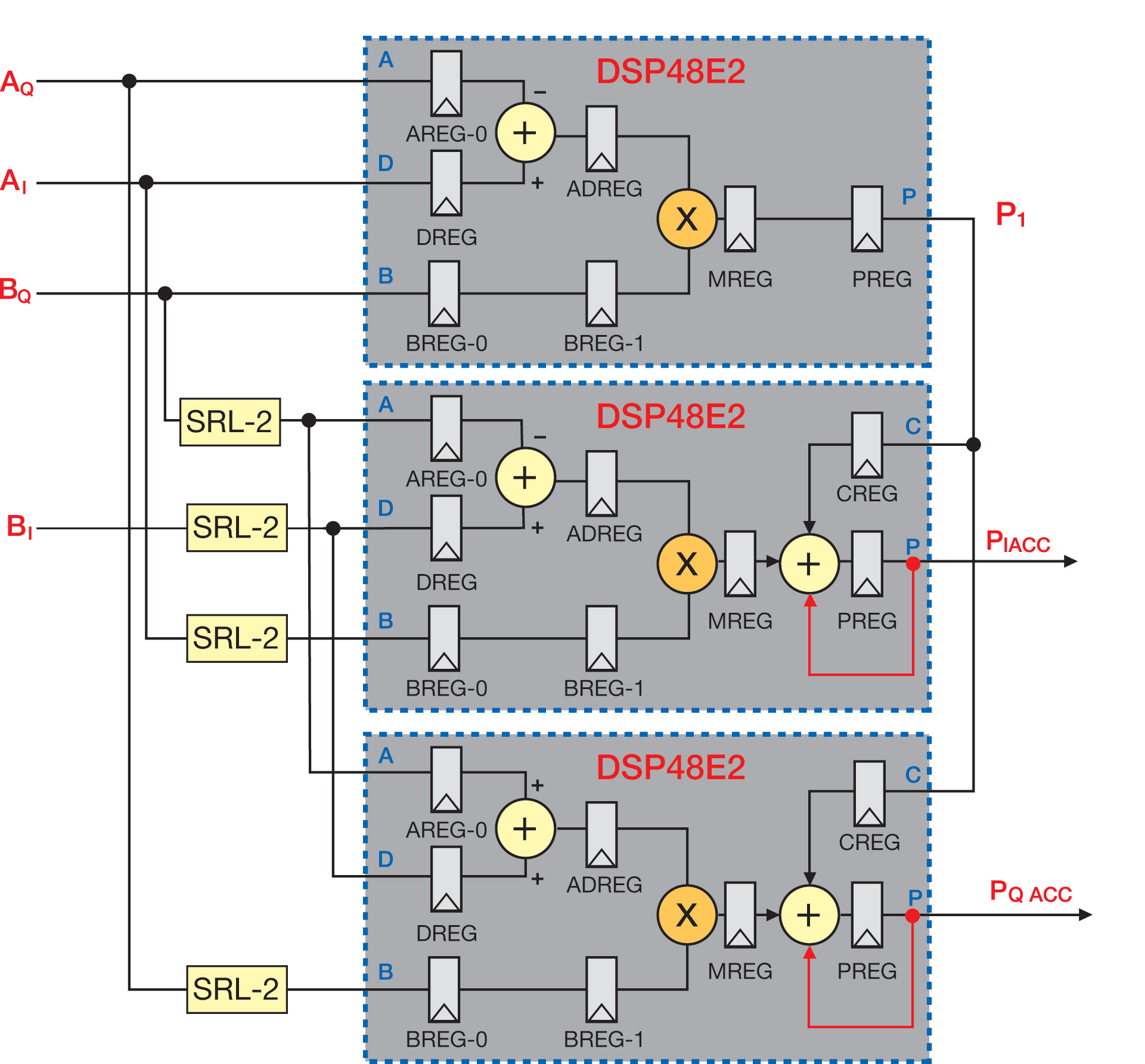
Figure 3 - Implementation of a complex MAC on 7 Series and UltraScale architectures
The complex MAC is finally completed by adding an accumulator on each of the PI and PQ outputs. Again this accumulator works on large data widths and is therefore better integrated within a DSP48 slice. The corresponding implementation for an UltraScale device is shown in Figure 3, which demonstrates the benefit of the W-mux integration. The PI and PQ DSP48E2 slices absorb the accumulators, with 40% resource savings. It is worth mentioning that the latency is also reduced, which may be beneficial for some applications.
Using a similar construction, you can build a complex filter (one with complex data and coefficients) with three real filters, as depicted in Figure 4. The real and imaginary parts of the input signal are fed into two real filters, with coefficients derived respectively as the difference and sum of the imaginary and real parts of the filter coefficients. The third filter processes the sum of the input real and imaginary parts in parallel, using the real part of the coefficients.
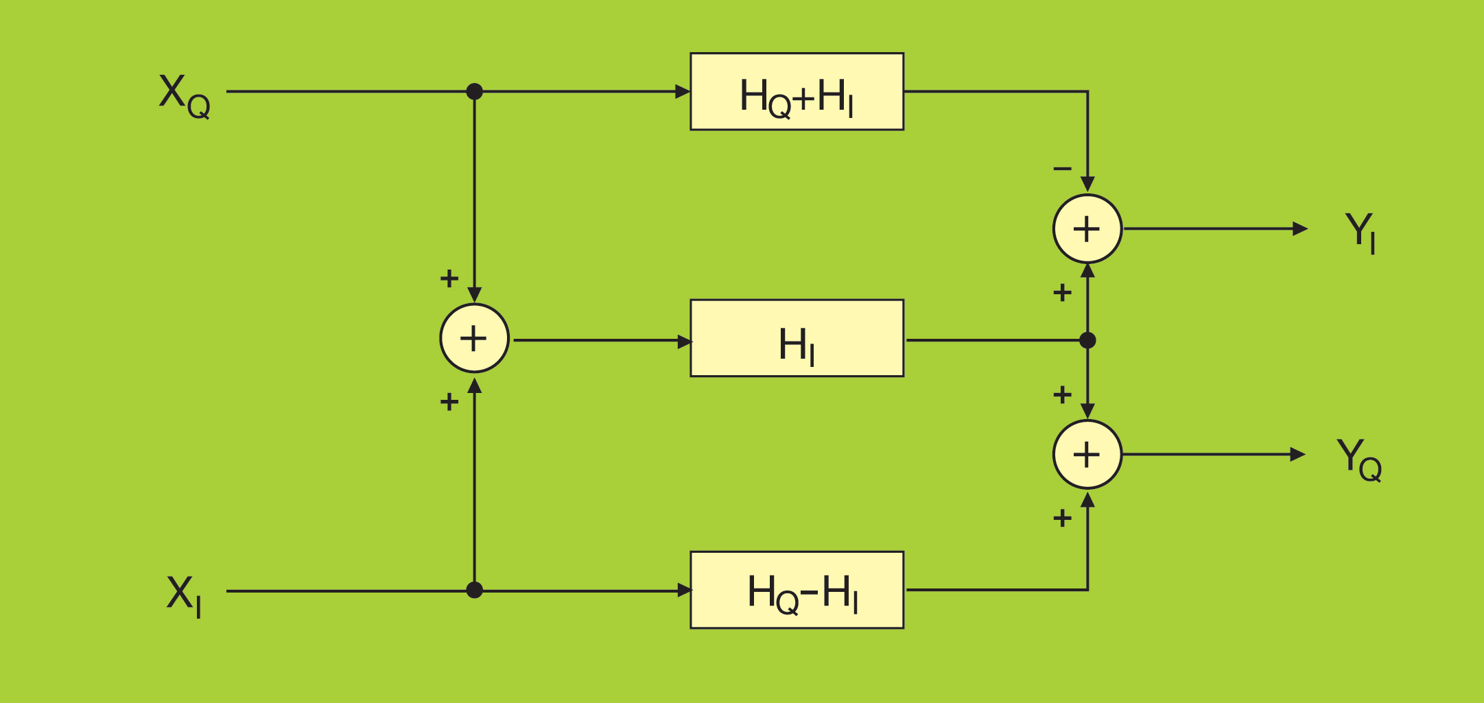
Figure 4 - Implementation architecture of a complex filter
The outputs of these three filters are finally combined to generate the real and imaginary components of the output, which can again benefit from the W-mux, when parallel filters need to be built, which is typically the case for the equalisers used in DFE applications.
This article was edited from the original by Philip Ling, Editor, Electronic Specifier Design. The original article can be viewed here.
Product Spotlight
APV1111GVY
Panasonic

Panasonic PhotoMOS® Photovoltaic MOSFET High-Power Drivers
| SKU: | |
|---|---|
| Stock: | 3490 |
| Cost: | $3.95 |
