Protecting wearable electronics from the human body
Wearable electronic devices are presenting new challenges to circuit protection technology, says Adam Chidley, European Product Manager, Avnet Abacus.
The human body is one of the biggest enemies of circuit protection for modern portable electronic devices, because of ESD.
ESD can mean extremely large voltages experienced by the device when it’s touched by the user. For devices such as smart watches and smart glasses, which are typically in close contact with the body, this is a particular concern. The IEC61000-4-2 model for real-world ESD events models ESD events between 2 and 15kV, which could obviously be extremely damaging for sensitive low-voltage ICs inside a small electronic device, even catastrophically damaging. Smaller manufacturing geometries, combined with a reduction of on-chip protection, have made today’s complex silicon devices more susceptible than previous generations. Clearly, ESD protection is required for all handheld electronic devices, but wearables present particular challenges, which will be discussed in detail in this article.
System-level vs. device-level
The first step to selecting circuit protection for any device is to study the application and understand what kind of ESD strikes the system may be subject to. For example, it’s unlikely that a smart watch would be expected to survive a direct lightning strike (though significant voltages are induced by lightning’s magnetic field in things like power cables, even when not directly struck). However, the smart watch will be in contact with body surfaces as a matter of course, so will be subject to ESD. See figure 1 for a comparison of lightning and ESD strikes.
 and ESD (bottom) strikes.jpg)
Figure 1 - Lightning (top) and ESD (bottom) strikes. Lightning transients have a rise time in the range 1.2 to 10μs and the duration is 50 to 1,000μs (between 50% of peak values). ESD is much shorter, with a rise time around 1ns and an overall duration around 100ns. (Image courtesy of Littelfuse)
Consumer devices are designed to withstand ESD strikes as per the standard IEC61000-4-2; this system-level model of real-world ESD events describes levels of strikes between 2 and 15kV, lasting 150ns with a rise time of less than 1ns and with a peak current of 7.5A (at 2kV). The system has to withstand 20 of these events to pass the test to the specified level for contact discharge or air discharge. These test criteria may seem stringent, but considering simply walking across carpet can generate a static voltage of 1.5kV (at relative humidity 65-90%), they are realistic. In fact, walking on carpet can generate much more static electricity in environments where the relative humidity is lower, in the region of 35kV for extreme cases.
Other ESD models exist, such as the Human Body Model (HBM); don’t fall into the trap of thinking that protecting your wearable device to this model will be enough to pass IEC61000-4-2. In fact, the HBM (as well as the machine model, MM, and the charged-device model, CDM) are derived from an old MIL-STD test setup which is intended for device-level protection in the manufacturing environment. That is, it describes how much individual ICs should be able to withstand when being handled by a person during the manufacturing process - this is as little as 500V since the devices are handled in an environment which is tightly controlled to reduce the chance of ESD strikes. It is not comparable to the model described by IEC61000-4-2.
Protecting wearables
Knowing a little more about the ESD environment in which the wearable device will be, next we will consider potential entry points for the ESD strike and how to protect them. ESD typically enters the system through any conductive interface that could be touched by the user, such as the touch screen, connectors, or any buttons and switches preset. The majority of ESD entry points may be protected by Transient Voltage Suppression (TVS) diodes; these diodes are specially designed to protect ICs by suppressing high voltage transients as they can respond (change state) very quickly to block overvoltage conditions. For example, both the Murata LXES series of ESD suppressors and TDK’s CTVS surge protection series offer response time of less than 1.0ns. TVS diodes are thus able to effectively clamp the voltage seen by the rest of the system at very low levels while experiencing large ESD strikes.
For things like buttons and switches, where data is not transmitted, high capacitance TVS diodes (order of tens of pF) can be used. The same goes for power connectors, which carry low voltage DC; higher capacitance TVS diodes are fine.
For connectors where there are low frequency signals, perhaps for a headphone jack, which carries audio signals where the highest frequency is around 20kHz, TVS diodes around 20pF should still be OK. For example, Bourns CD0603 bidirectional TVS diodes come with capacitances of 15, 12 or 10pF (for 5, 12 and 24V versions, respectively).
For connectors that carry high speed data, the situation is a little more demanding. High data rates for signals like USB 3.0 mean the capacitance has to be carefully considered, and in most cases, the lowest possible capacitance TVS diodes should be specified to avoid any affect on signal integrity. TE Connectivity’s ChipSESD series of devices offers input capacitance as low as 4.5pF and are bidirectional, easing the need for correct orientation during placement.
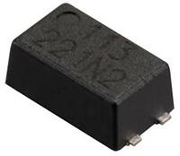
Small form factors are one of the biggest challenges when designing for compact wearable electronic devices. Thankfully, better fabrication processes allow TVS diodes to occupy the minimum of board space without compromising on protection. For example, AVX’s StaticGuard series of multilayer ceramic TVS diodes comes in sizes down to 0402 (1.0x0.5mm footprint). These devices also offer relatively low leakage current, 10µA, important for wearable devices with small batteries.

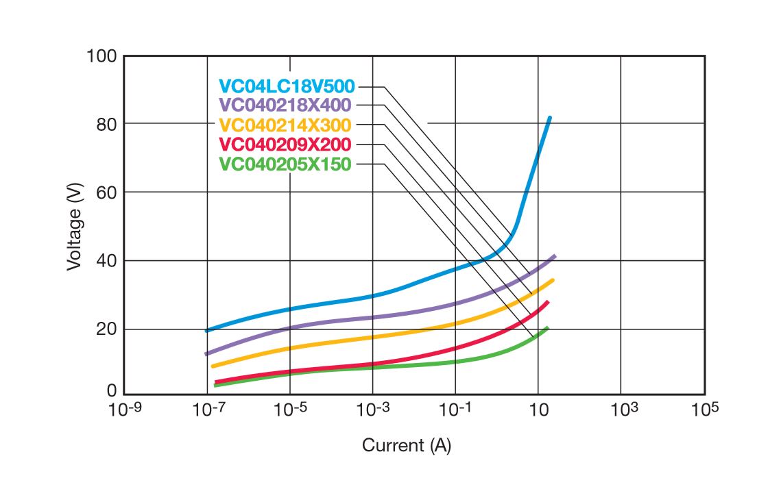
Figure 2 - AVX’s 0402 StaticGuard transient voltage suppressors exhibit excellent performance up to 20A peak current, while maintaining low DC leakage. (Image courtesy of AVX)
Good design practice
When designing any electronic system, it pays to think about how the device will withstand ESD events from the start of the design process. TVS diodes need to be placed as physically close as possible to any potential entry points for transients, such as switches, touch screens and connectors, so that any stub traces are as short as possible. This can affect subsequent layout steps so it’s worth considering early in the layout process.
Designers may not perceive that ESD protection adds value to their product as it is not contributing directly to any features. ESD protection is thus often ignored until the system has failed testing and remedial work needs to be undertaken. However, with an understanding of the importance of correct ESD protection and some sensible planning, the time and expense taken for remedial work can be avoided.
A wide variety of TVS diodes is available that suits compact portable devices such as wearables, including those with very fast response times, very low capacitances for signal integrity, plus small case size and low leakage current.


