
Building wearables that sense, think, and communicate: part 1
The design requirements for modern wearable products include sleek design, embedded intelligence, energy efficiency, expandability and cost-effectiveness. These create many design challenges for manufactures of these types of devices. The pressure from never-ending improvement forces designers to look for ways to integrate more functionality into a single chip to simplify design.
Here, Jaya Kathuria and Anbarasu Samiappan explain how engineers can use feature-rich MCUs to meet the design challenges of building interactive wearables devices.
Design challenges of next-gen smart wearables:
The demand for more features means development cycles have also significantly been reduced. Developers must be able to adapt to changes in requirement on a regular basis. Meaning it is critical to have a platform that is versatile and can provide key features such as low power, small form factor and high-speed computing. Figure 1 shows the glance of the design challenges in modern wearable products.
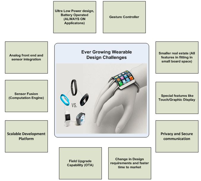
Figure 1: Quick Glance – Wearable design challenges
Always ON applications and power implications:
One of the critical requirement for wearables is the continuous monitoring of various sensors. This imposes the requirement that processors be 'ALWAYS ON' to monitor sensors and process this information. For example, motion sensors and pressure sensors are used to implement a pedometer. The pedometer needs to continuously count steps and report them to a wearable display or mobile app via a wireless channel. Most wearables devices rely on batteries or energy harvesting to power them through the day. This means engineers need to be extra cautious in designing even the smallest of power extravagances into a product. To ease this design constraint, power- and area-efficient MCUs are needed for the wearable or IoT application.
One effective way to handle power efficiency is to utilise the flexible power modes of your MCU and its ability to schedule individual system events in appropriate power modes. This allows you to achieve optimum power consumption based on the primary use cases for your application. You can approach the problem with a power budget broken into specific tasks or circuit blocks. By basing allocating the power budget per task or circuit, you can find more flexibility when it comes to defining the power consumption of the components you need. For example, an MCU like the PSoC4-BLE from Cypress offers multiple system power modes including Active, Sleep, Deep-Sleep, Hibernate, and Stop. With current consumption as low as 60nA in Stop mode, you can optimise power consumption for your application.
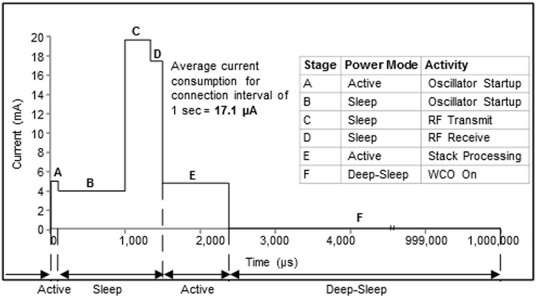
Figure 2: Power profile in different power modes (Example: PSoC4 BLE)
Analogue front end and sensor integration:
Put simply wearables are nothing but a cluster of sensors with a CPU and wireless link. Wearables typically offer features like, health monitors and fitness trackers by sensing various physical signals like pressure, motion, position, touch, heart rate and pulse rate. Eventually each of these sensors, whether it is analogue or digital, needs a front end circuit for interfacing to the MCU.
An Analogue Front End (AFE) is signal-conditioning circuitry that uses sensitive analogue circuits to process the sensor output as the output from the sensors cannot be used directly with the MCU. The AFE acts as an interface between the sensor and processing unit. A sensor interface circuit will require a biasing circuit, an amplifier, comparators, Digital to Analogue Convertor (DAC), analogue multiplexers, voltage references, a filter network for noise suppression and error suppression techniques like offset removal, and an Analogue to Digital Converter (ADC) to digitise and process the sensor data. A system designed with a traditional microcontroller available on the market today will require the above mentioned circuit to be built outside the chip, although some may have a fixed-function ADC integrated into the MCU. For digital sensors that provide their output in a digital stream, a communication port like I2C, UART, or SPI is required to connect the digital sensor output to the MCU.
Consider an Activity monitor as an example to understand the Analogue Front End (AFE) and Digital Front End in a wearable system. Figure 3 depicts a block diagram which is a complete system of an Activity monitor using a single SOC. On the analogue side, the iDAC component is used to excite the Thermistor to sense the temperature. The voltage drop across the Thermistor, which represents the temperature, is connected to the on-chip SAR ADC thorough an Analogue multiplexer. The ADC converts the analogue voltage into digital counts, which can then be processed by the CPU. The on-chip reference voltage block, Vref, is used to generate a fixed analogue voltage reference for the accurate measurement of data. Also, a capacitive sensing mixed-signal component is employed to enable user presence detection. Capacitive sensing also allows designers to replace mechanical buttons with a sleek user interface built on touch and proximity. The ambient light sensor is enabled with op-amps and voltage references along with an external photodiode. The reverse bias current of the photodiode varies with the incident light intensity. The differential Trans-Impedance Amplifier (TIA) converts the photodiode current into a voltage.
On the digital side, a Digital Sensor Accelerometer is used to implement a pedometer. A pedometer counts the number of steps taken by the user and also calculate the number of calories burned in the process. Pedometers use accelerometers to detect patterns of changes in acceleration to detect a step. By using an accelerometer sensor along with an additional altimeter sensor in the system, the total number of calories burned by the wearer can be calculated.
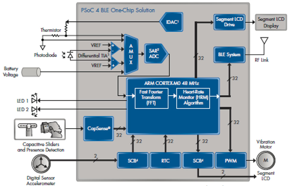
Figure 3: Activity monitor example (PSoC4 BLE)
Board or system real estate:
Wearables are often small, sleek electronic devices, and there is a clear need to densely pack the electronics so that they occupy minimal space whilst at full functionality.
These factors force designers to maximise integration of functionality, MCUs like the PSoC4-BLE2 makes greater system integration possible. For example, SOCs can integrate Analogue Front Ends for sensor interfaces, computing engines like an ARM CPU for sensor fusion, on-chip memory, wireless connectivity like Bluetooth Low Energy, and capacitive touch capabilities to support innovative interfaces. This enables product designers to build compact, small form factor designs for the next-gen of portable and wearable applications.Such feature integrations in a single chip not only reduces the board space needed, it also brings down system cost and power. A representation of the various function integration in a single MCU/SoC is shown in Figure 4.
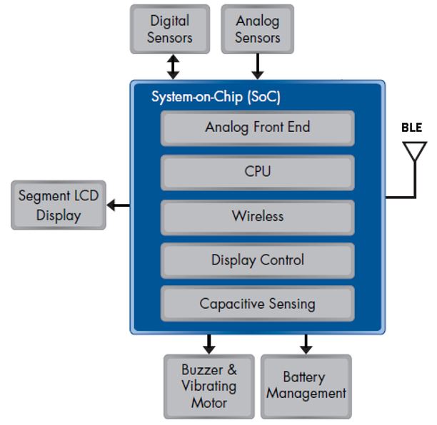
Figure 4: Functional integration in MCU/SoC
Once features are integrated, the next task for a designer is to choose an MCU/SOC that offers all these features in a tiny footprint that meet their needs for smaller form factor. Wafer-Level Chip-Scale Packaging (WLCSP) offers an efficient way to bring a great deal of functionality into a small chip size, unlocking the potential of the next-gen wearable products (see Figure 5).
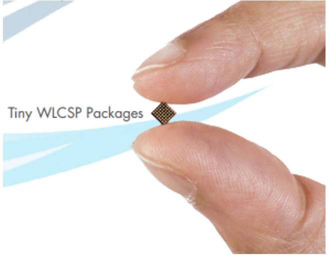
Figure 5: Tiny Form factor of MCU/SoC
Sleek User Interface (Gestures):
Given the small size of wearable devices, it is important to provide an easy way for users to communicate with their devices. This can be done by including a small number of User Interface (UI) options within the device, and also by connecting the wearable device to an extended device e.g. a smartphone for a full-featured user interface.
Accessibility to the technologies like capacitive touch sensing have made it possible to implement smart gestures in wearable devices. Capacitive touch can be introduced either as standalone touch silicon or as an integrated featured of an MCU/SOC. Gesture capabilities not only simplify the UI but also enable lower operating power since the device can be wakened upon a specific user gesture.
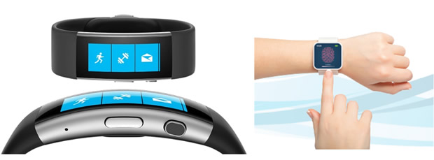
Figure 6: Gesture enabled: in Tiny screen Figure 7: Wake-on approach gesture
Privacy and secure communication:
With the rapid growth of the wearable technology market, Bluetooth Low Energy (BLE) has become the main wireless standard for all kinds of devices, from smartwatches to beacons to connected cars. The BLE protocol has to be carefully handled by the designers to avoid potential security vulnerabilities in data communication over wireless link. The latest updates to the BLE protocol comes equipped with several security and privacy capabilities to cover the encryption, trust, data integrity and privacy of the user’s data. For example, the BLE link layer provides various encryption algorithms like CRC and AES for robust and secure data exchange over BLE. There are also BLE modules that can provide additional security and privacy features to make BLE technology an even stronger wireless solution for those applications which need it.
In Part 1, we have discussed several design challenges of wearable product design, including Always-ON applications and power implications, analogue front-end and sensor integration, board or system real estate, sleek user interface through gestures, and privacy and secure communications. In Part 2, we will cover more design challenges like Field Upgrade capabilities (OTA), energy harvesting, connectivity (BLE, ZigBee, WiFi), and special features such as Wrist Detection, Capacitive Touch Siders and Buttons, Capacitive Touch Screens, water tolerant design and Segment LCD Drive.
Product Spotlight
APV1111GVY
Panasonic

Panasonic PhotoMOS® Photovoltaic MOSFET High-Power Drivers
| SKU: | |
|---|---|
| Stock: | 3490 |
| Cost: | $3.95 |
