Design
Radio without limits
Integrating miniature low noise amplifiers in handsets can be an effective solution to a growing design dilemma for OEMs embedding FM radio receivers. Houssem Chouik, Product Marketing Manager RF Transistors at Infineon Technologies, discusses this.
FM rHowever, by employing so-called ‘active antenna’ techniques, where a suitable low-noise amplifier (LNA) is directly interfaced to the electrically small integrated FM antenna, much of the FM receiver’s sensitivity may be regained. So-called active antenna modules containing a unique passive structure tailored for FM radio and directly interfaced to appropriate amplifier circuitry are rapidly gaining market acceptance in emerging mobile device applications. High gain, low noise amplifiers with small footprints and high robustness against Electrostatic Discharge (ESD) are key components for these active antenna designs.
##IMAGE_2_C##
Figure 1: BGB719N7ESD needs less board space and external components as compared to its predecessor (BGB717L7ESD).
Design challenges for embedded antennas
While providing several benefits, the active antenna design has its challenges. Two problems arise when integrating the antenna inside the phone. First, electrically small and low-profile antennas have high input reactance, low input resistance, and low radiation efficiency, making them difficult to impedance-match to other circuit elements. The second problem relates to isolation from transmitting antennas co-located with the FM antenna inside the phone. It is in effect the RF currents on the chassis that are responsible for most of the radiation. Any other antenna connected to the chassis, or which similarly relies on the chassis as the main radiator, will therefore experience very high levels of signal leakage.
An electrically small, reduced-size embedded antenna results in significantly reduced antenna gain and consequently low receiver sensitivity compared to the external headset cable antenna. To compensate against this degraded sensitivity, an active antenna topology has to be used.
In addition to the LNA as a key component of an active antenna system, in most cases external ESD protection is also required, along with an SPDT switch for antenna diversity switching, which permits the mobile device to switch between a wired external headset and an internal embedded antenna.
##IMAGE_3_C##
Table 1: Electrically short antenna designs require LNA
Using a high performance LNA will increase the receiver sensitivity. However, there are some challenges in the design of an optimal LNA for this purpose. In cellular phones, very low current consumption for longer battery lifetime is required, which is in direct opposition to the high linearity requirements for the LNA. Other requirements on the LNA include a power-off function, high ESD robustness at the RF-in port, very small dimensions and low external part count.
Shrinking the size of an embedded antenna introduces a high loss in the system which deteriorates the receiver performance, namely the receiver sensitivity. Usage of a low noise amplifier in conjunction with a co-developed antenna radiator can solve this problem by enhancing the receiver sensitivity. Due to the very small size, the antenna impedance is very high and thus the LNA has to be matched to this high impedance and in addition offer a low noise figure. Using it in a handheld device also demands low current consumption, power-off function and high linearity due to the co-existence of cellular band transmitters within the same handset. The LNA has to be designed for worldwide FM band (76-108MHz) and high ESD robustness at the RF-in port, to support outstanding ESD robustness requirements on the system level.
Infineon’s latest generation LNA is able to solve the main problems in embedded active FM antenna designs for handset devices enhancing the receiver sensitivity and consuming less power and less board space. The BGB719N7ESD is an advanced LNA MMIC specifically designed for FM antenna systems requiring high gain, low noise figure, high ESD robustness, reduced power consumption and low distortion. The device is based upon Infineon Technologies cost effective SiGe:C technology.
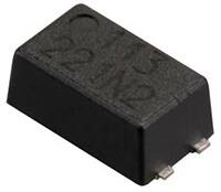
The BGB719N7ESD fulfils all the mentioned performance criteria in a very small and leadless TSNP-7-6 package (1.26mm x 1.4mm x 0.31mm). The integrated active biasing enables a consistent DC operating point with varying temperature and over process variations. The product finds application in all kinds of mobile devices such as mobile phones, PDAs, portable FM radio and MP3 players.
Compared to the previous generation device (BGB717L7ESD) the new BGB719N7ESD provides several enhancements in a typical FM radio application, including smaller footprint dimensions (6mm2 compared to 20mm2), higher gain (23dB versus 21dB), reduced supply current (Icc = 2.8mA compared to 3.0mA), higher stability and fewer external passive components (3 versus 7).
The BGB719N7ESD provides integrated, on-chip ESD protection sufficient for ESD strikes up to 2kV (HBM). Adding Infineon’s ESD protection diode ESD0P8RFL in front of the LNA improves the system’s ESD performance up to 8kV contact discharge per IEC61000-4-2 at the RF input pin. The external ESD protection diode is mounted in the small leadless TSLP-4-7 package (1.2mm x 0.8mm x 0.39mm) and has a parasitic capacitance of only 0.8pF.
##IMAGE_4_C##
Figure 2: Compared to the previous generation (BGB717L7ESD) the new BGB719N7ESD provides several enhancements in a typical FM radio application, such as higher gain.
With this application proposal Infineon offers a perfect solution for an ESD robust LNA for embedded FM radio antennas in handsets. The design is suited for miniature and slim handset design due to the small form factor of the TSLP packages. The LNA fits easily into an 8mm x 8mm sized area when using 0402 capacitors. The application circuit using the BGB719N7ESD requires minimal usage of external SMD components due to the integrated DC bias circuit which shrinks required PCB space and thus reduces overall cost.
The BGB719N7ESD can be easily matched to electrically short half-loop antennas and monopole antennas. Therefore a single passive element needs to be placed at the input of the LNA. In case of a half-loop antenna a shunt capacitance in the range of 30pF is needed. If the application uses a monopole antenna, a shunt inductance in the range of 300nH is required.
To get immediately started with the BGB719N7ESD design the device is available in volume, supported by evaluation boards and comprehensive documentation. In addition system designers can get all key components for high performance embedded antenna applications from one single source, including LNA, ESD protection diodes and CMOS switches.
Key features of the BGB719N7ESD include:
-Worldwide FM band support (76 to 108MHz)
-Low external parts count (only 3 external capacitors required)
-Super miniature low profile leadless package TSNP-7-6
-High gain at only 2.8mA current consumption
-Integrated active biasing circuit enables stable operation point against temperature, supply voltage and process variations
-Integrated ESD protection for all pins (1.5kV per Human Body Model ‘HBM’)
-High input compression point (IP1dB = typ. -6dBm)
-High input impedance
-Excellent noise figure from latest SiGe:C technology (1.2dB)
-Wide operation voltage: 1.5V to 4.0V
-Power-off function
-Pb-free (RoHS compliant) and halogen-free (WEEE compliant) product


